
Building a Basic CPU Simulator with TkGate on Linux: A Journey into Computer Architecture
This a basic CPU-Simulator where you can run some simple Assembly Language like code and get the desired output. This project is made using TkGate.


Introduction
In this blog post, I want to share a small project I worked on during my 2nd year of the BTech CSE Program in the Computer Architecture and Organisation Lab Assignment. I created a Basic CPU Simulator capable of running code similar to assembly language. To build this simulator, I utilized the TkGate application, which is available on Linux operating systems.
My project drew upon my understanding of essential processor components such as the Program Counter, Registers, and the Arithmetic Logic Unit (ALU). With these components, I was able to design and implement various programs, including tasks like checking whether a number is prime or finding the maximum sum of consecutive numbers.
I'll take you through the process of creating this simulator and provide insights into how it functions and the programs I developed using it. So, let's dive in and explore!
Code and Designs
GitHub Repository : https://github.com/Shreyansh-Agarwal2022/Basic-CPU-Simulator (it contains files of my project)
ISA Design PDF : https://drive.google.com/file/d/11RK7gVg6CY0g964Xu_yrfCuIogQMcH9R/view
Demo Video :
Code in the example above : (the code is a little bit changed, in this code didn't check condition of the number is 1 or not because 1 is not prime)
Prerequisites
You should have studied Computer Architecture Course.
TkGate can only on the Linux operating system.
You have to install TkGate by writing the following command in the terminal
sudo apt-get install tkgate.An effort to learn something new 🙂.
Cracking the Code: A Deep Dive into Instruction Writing
The instruction length is 16-bit in my project and it is divided into :
0 to 7 : Immediate Value (8-bit)
5 to 7 : Register 2 address (3-bit) (only input is stored here)
8 to 10 : Register 1 address (3-bit) (both Input and Output is stored here)
11 : Addressing Mode (1 for immediate, 0 for register 2)
12 to 15 : Opcode (4-bit)
Data is 8-bit in my project.
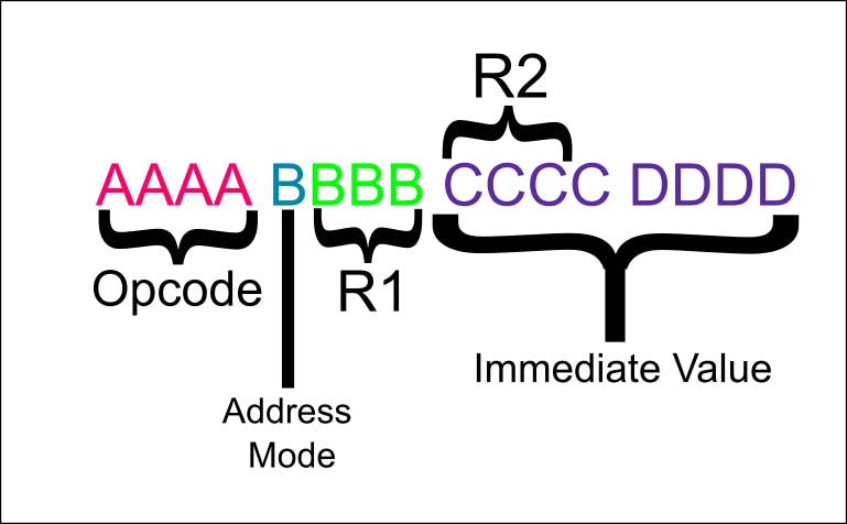
Here, R1 and R2 represent the addresses of Register 1 and Register 2 within our instruction format.
In my project, the instruction format is constrained to a maximum of 16 instructions due to the 4-bit opcode, allowing for a maximum of 8 registers as the 3-bit addressing mode determines the register address. Additionally, a single bit is dedicated to the addressing mode.
The register R1 is the source and destination register in most of the instructions. Refer to the PDF Document.
When the Addressing mode bit has a value of:
1: Immediate value is utilized, and R2 is disregarded. 0: R2 is utilized, and the Immediate value is disregarded.
To understand which opcode values correspond to specific operations, please refer to the provided PDF document. There I had explained every instruction briefly.
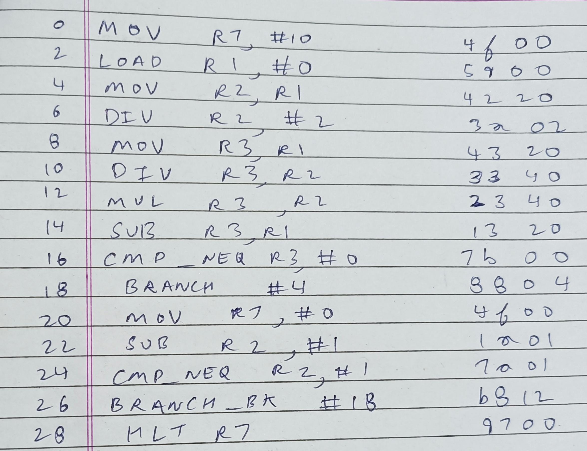
Now, let's explore the process of designing instructions with some practical examples (here [Rx] means 8-bit value in register Rx) :
MOV R7,R3 : 0100 0111 0110 0000
Here, the Opcode of MOV is 0100, the addressing mode in register-register is 0, the R7 address is 111, the R3 address is 011 and the remaining last 5 bits are useless so you can write anything, let it be 00000.
In this MOV we will do [R3]->R7
MOV R0,#10 : 0100 1000 0000 1010
Here, the Opcode of MOV is 0100, the addressing mode in register-immediate is 1, the R0 address is 000, and the immediate value to represent 10 in 8 bits is 0000 0101.
In this MOV we will do 10->R7
SUB R4,R3 : 0001 0100 0110 0000
Here, the Opcode of SUB is 0001, the addressing mode in register-register is 0, the R4 address is 100, the R3 address is 011 and the remaining last 5 bits are useless so you can write anything, let it be 00000.
In this SUB we will do [R4]-[R3] -> R4
CMP_EQ R1,#0 : 0110 1001 0000 0000
Here, the Opcode of CMP_EQ is 0110, the addressing mode in register-immediate is 1, the R1 address is 001, and the immediate value to represent 0 in 8 bits is 0000 0000.
In this CMP_EQ we will compare if [R1] and 0 are equal or not and give output in 1-bit value (if equal then 1 else 0). It doesn't save value in any register in the register file but in the flag register.
BRANCH_BK #12 : 1011 1000 0000 1100
Here, the Opcode of BRANCH_BK is 1011, the addressing mode is immediate so it is 1, R1 doesn't matter here so let it be 000, and the immediate value is 12 to represent it in 8-bit we write 0000 1100.
BRANCH_BK will only work when the flag register has 1 in it after comparing instructions. It will subtract value 12 from the current value of the Program Counter(PC) register. Eg. the current value in the PC register is 38, then this branch instruction will make the PC register value equal to 26. BRANCH adds value to the PC register current value.
HLT R7 : 1001 0111 0000 0000
Here, the Opcode of HLT is 1001, the addressing mode is 0, the address of R7 is 111, the R2 doesn't matter here so let it be 000, and the remaining 5 bits don't matter so let it be 00000.
HLT will stop the PC register from updating and that stops our whole program. In the end, we can also see the value of R7.
Hopefully, now you will be able to write your instructions.
Note : After writing the instruction in binary convert it to hexadecimal because in instruction.mem file we write instructions in hexadecimal. You can convert binary to hexadecimal using this website.
Look at this instruction.mem file below
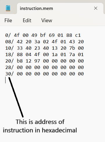
In our setup, we expressed instructions in hexadecimal format. Each row contains four 16-bit instructions. To illustrate, the first row follows this pattern: "4f 00" represents the first instruction located at memory address 0, "49 bf" signifies the second instruction at address 2, "69 01" indicates the third instruction at address 4, and "88 c1" designates the fourth instruction at address 6. Likewise, in the second row, "42 20" denotes the fifth instruction positioned at memory address 8, and this pattern continues for subsequent instructions.
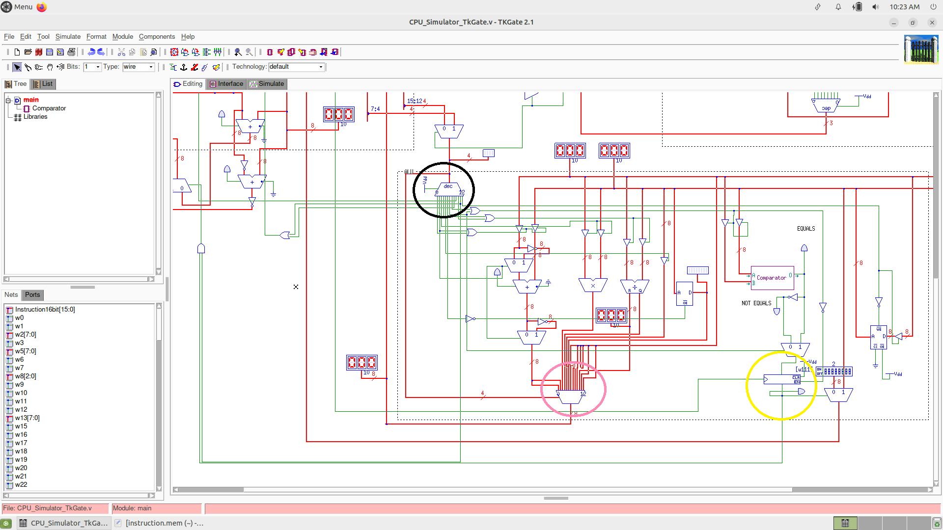
The Inner Workings of the Circuit: A Comprehensive Breakdown
Let's start with the easiest part the comparator.
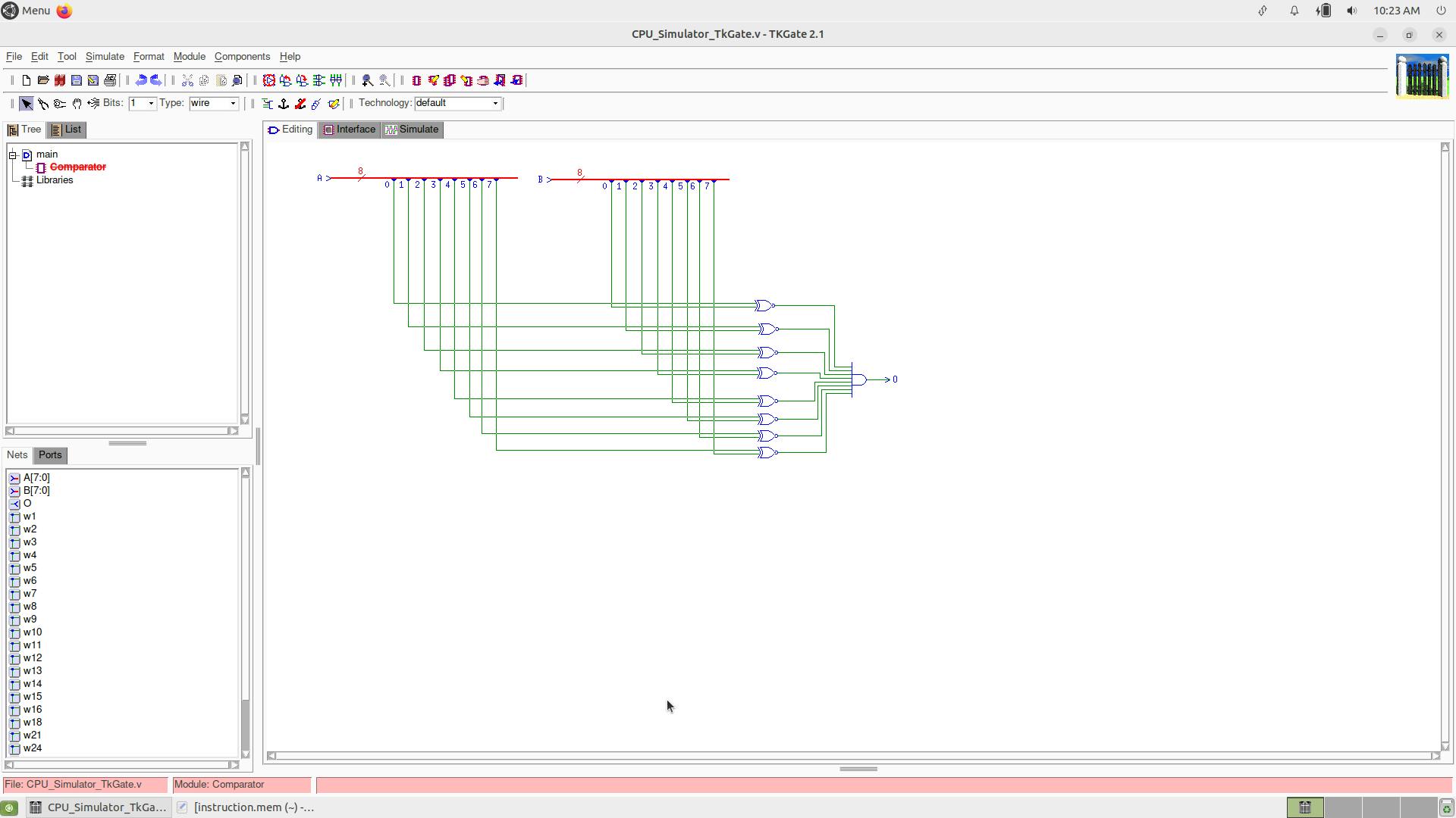
In this, the comparator has two types of gates XNOR and 8 input AND gate. XNOR gate compares each bit of input A and B in this module and the 8 input AND gate checks if all bits coming out from all XNOR gates are 1 or not. XNOR gives 1 where both input bits are the same or not.
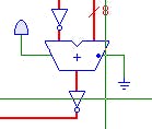
Let's understand the register file

Let's understand it by each circled part :
The blue circled component signifies the CLR (clear) switch, which should always remain in the ON position. It's only turned OFF when a complete reset of all registers is required.
Within the red circle, you'll find the component responsible for selecting the source register R2. This selection is accomplished by instructing the multiplexer through the select line to use the desired register's address.
The yellow circled component facilitates the retrieval of data from source register R1. Similar to the selection of R2, the select line of the multiplexer is used to specify the address of the register containing the data.
Encircled in pink is a 2-to-1 Multiplexer, responsible for determining which value serves as the source data in our instruction. The addressing mode bit acts as the select line for this multiplexer, making the choice.
The green circled section serves the purpose of enabling destination register R1. It employs a 3-to-8 decoder with the input being the address of register R1. Once the desired register is enabled, it can be updated with new values as needed. Here, the destination register and the source register are the same (R1).
To understand how registers work in TkGate, you can make your small circuit and by a hit-and-try method, try to understand it properly.
Now, let's move to the ALU part
As you go from left to right in this ALU circuit, we go top to bottom from the ISA Design PDF, let's understand this part :
Encircled in black is a 4-to-16 decoder with its input line being the opcode section of our instruction set. It plays a pivotal role in decoding and routing instructions.
Within the pink circle, you'll find the component responsible for choosing the data path to send to the destination register. It employs a multiplexer with the 4-bit opcode serving as the select line for this critical decision.
The yellow circled portion represents the flag register, which serves as the repository for the output of the comparator, holding valuable information about the state of the circuit.
Take a closer look at the Subtractor circuit illustrated below in TkGate:
Now, let's move on to the hardest part of our circuit, the Program Counter.
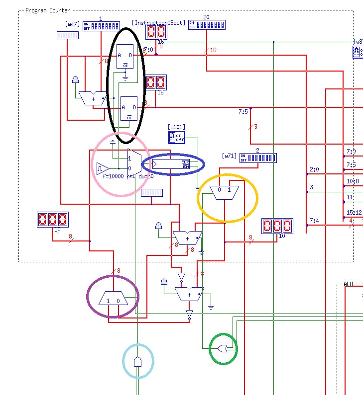
Let's understand this circuit part by part :
The black circled part is used to read instructions from memory, since our instruction length is 16-bit we use two RAM components of output data as 8-bit each.
The pink circled part is a MUX which selects the clock, when the program comes to HLT (halt) instruction, we make the clock as ground. I increased clock frequency from 100 to 10,000 because of the overall delay in the ALU and register file.
The green circled OR gate is used to choose offset when we have Branch instructions in the yellow circled MUX.
The cyan circled AND gate is used to select Adder or Subtractor in the violet circled MUX.
The navy blue circled part is the PC register in which we stored the memory address of the current instruction.
Hopefully, you were able to understand the Program Counter functioning.
Exploring Project Challenges and Limitations
When we simulate this circuit we get some time violations errors and runtime errors. This is because of how TkGate writes in memory (in which we use ROM).
I hadn't made a better comparator with less than and greater than functionality. So, I took the help of my friend and he made a comparator in this circuit.
While making the circuit in TkGate it randomly crashes, so keep saving files every 5 minutes.
TkGate is limited to Linux only. I used an Oracle virtual machine to use Linux for TkGate
Conclusion
In conclusion, this project has been a fascinating exploration of the world of CPU simulation, instruction design, and circuit mechanics. We've taken a closer look at the intricacies of the components, from the Program Counter to the decoder and multiplexers, to understand how they work together to execute instructions.
While the journey has had its share of challenges and limitations, it's been a valuable learning experience. We've deciphered the complexities of instruction writing, addressed anomalies, and gained insights into the inner workings of our circuit.
I hope this blog has provided you with a deeper understanding of the project and ignited your curiosity about computer architecture. Thank you for joining me on this learning adventure, and I look forward to sharing more insights in the future. Happy coding and exploration! 🚀🧠
Thank you for reading to the end! 🙌 I hope you found this journey of learning enriching and enjoyable.
You can contact me on Twitter(𝕏).